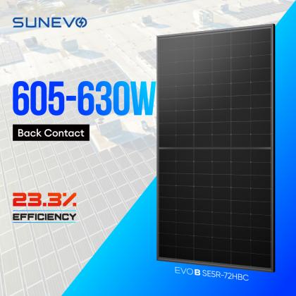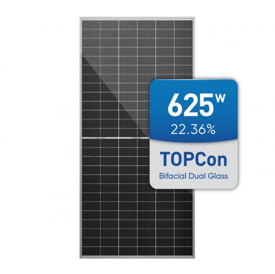
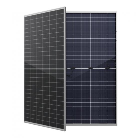
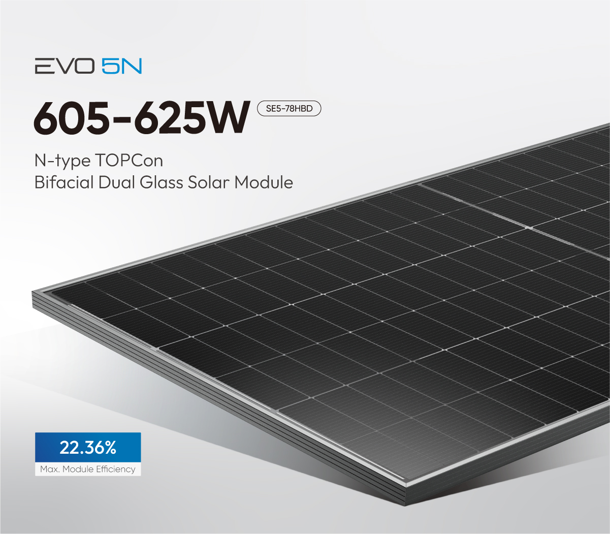
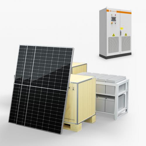
EVO 5N Series Bifacial modules combine leading N-type TOPCon technology, 182mm silicon wafer, and half-cell. 30 years lifespan brings 10-30% additional power generation compared with conventional P-type modules. The SunEvo N-type Bifacial Half-cell Module can reach a power output range between 605W to 625W.
Brand:
SunEvoPower Range:
605W~625WMax. Efficiency:
22.36%Number of Cells:
156 (6×26)Dimensions of Module L*W*H:
2465 x 1134 x 30mmWeight:
34.5kgsFront Side Glass:
2.0mm coated semi-tempered glassBack Side Glass:
2.0mm semi-tempered glassFrame:
Anodized aluminium alloyJunction Box:
Ip68 rated (3 bypass diodes)Cable:
4mm² , 300mm (+) / 300mm (-), Length can be customizedWind/Snow Load:
5400PaConnector:
MC4 compatibleBifaciality:
80±5%EVO 5N N-type TOPCon 156 Half Cells 605W 610W 615W 620W 625W Bifacial Dual Glass Solar Module
EVO 5N Series Bifacial modules combine leading N-type TOPCon technology, 182mm silicon wafer, and half-cell. 30 years lifespan brings 10-30% additional power generation compared with conventional P-type modules. The SunEvo N-type Bifacial Half-cell Module can reach a power output range between 605W to 625W.
Electrical Parameters (STC*)
|
Maximum Power (Pmax/W) |
605 |
610 |
615 |
620 |
625 |
|
Maximum Power Voltage (Vmp/V) |
45.63 |
45.76 |
45.90 |
46.03 |
46.16 |
|
Maximum Power Current (Imp/A) |
13.26 |
13.33 |
13.40 |
13.47 |
13.54 |
|
Open Circuit Voltage (Voc/V) |
55.30 |
55.41 |
55.53 |
55.64 |
55.75 |
|
Short Circuit Current (Isc/A) |
13.97 |
14.04 |
14.11 |
14.18 |
14.25 |
|
Module Efficiency (%) |
21.64 |
21.82 |
22.00 |
22.18 |
22.36 |
|
Power Output Tolerance (W) |
0/+5W |
||||
|
Temperature Coefficient of Isc |
+0.045%/°C |
||||
|
Temperature Coefficient of Voc |
-0.250%/°C |
||||
|
Temperature Coefficient of Pmax |
-0.290%/°C |
||||
| 5% | Maximum Power (Pmax/W) | 635 | 641 | 646 | 651 | 656 |
| Module Efficiency STC(%) | 22.73 | 22.91 | 23.10 | 23.29 | 23.48 | |
| 15% | Maximum Power (Pmax/W) | 696 | 702 | 707 | 713 | 719 |
| Module Efficiency STC(%) | 24.89 | 25.10 | 25.30 | 25.51 | 25.71 | |
| 25% | Maximum Power (Pmax/W) | 756 | 763 | 769 | 775 | 781 |
| Module Efficiency STC(%) | 27.05 | 27.28 | 27.50 | 27.73 | 27.95 |
1. Texturing
The texturing section (a total of 6 lines) includes in turn
pre-cleaning
Pure water washing before velvet
Texturing*3
Pure water washing after velvet
after cleaning
After washing, wash with pure water
pickling
Pure water washing after pickling
slow pulling pre-dehydration
drying*5 etc.
2. Boron diffusion
The purpose of the diffusion process is to form a PN junction on the silicon wafer to realize the conversion of light energy into electrical energy. The PN junction manufacturing equipment is a diffusion furnace. The project uses gaseous boron trichloride to diffuse the silicon wafer in the diffusion furnace. Boron atoms diffuse into the silicon wafer and form a layer of borosilicate glass on the surface of the silicon wafer. The main reaction equation is:
4BCl3+3O2→2B2O3+6Cl2↑
2B2O3+3Si→3SiO2+4B
3. SE laser redoping
The laser doping technology is to do heavy doping on the contact part of the metal grid line (electrode) and the silicon wafer, while keeping the light doping (low concentration doping) outside the electrode. Pre-diffusion is carried out on the surface of the silicon wafer by thermal diffusion to form light doping; at the same time, the surface BSG (borosilicate glass) is used as a local laser heavy doping source. Through the local thermal effect of the laser, the atoms in the BSG rapidly diffuse into the silicon wafer for the second time to form a local heavy doping region.
4. Post-oxidation
Where the surface of the silicon wafer is treated by laser SE, the oxide layer on the boron diffusion surface (light incident surface) is destroyed by the spot energy of the laser. During alkali polishing and etching, an oxide layer is required as a mask layer to protect the phosphorus diffusion surface (light incident surface) of the silicon wafer. Therefore, it is necessary to repair the oxide layer on the surface scanned by laser SE.
5. POPAID deposition in-situ doping
The POPAID process is a key process for integrating the plate coating prepared by the tunnel oxide layer and the doped silicon layer.
6. Annealing
Place the silicon wafer in a reaction tube made of quartz glass, and the reaction tube is heated by a resistance wire heating furnace to a certain temperature (the commonly used temperature is 900-1200°C, and it can be lowered to below 600°C under special conditions). When oxygen passes through the reaction tube, a chemical reaction occurs on the surface of the silicon wafer:
Si (solid state) + O2 (gas state) → SiO2 (solid state)
7. BOE cleaning
Pickling tank*2
washed
After pickling (HCL/HF/DI)
washed
slow lifting
drying*6
8. Front coating
The basic principle is to use high-frequency photo-discharge to generate plasma to affect the film deposition process, promote the decomposition, combination, excitation, and ionization of gas molecules, and promote the generation of reactive groups.
The main chemical reactions that occur during PECVD deposition of silicon oxynitride films are:
SiH4+NH3+N2O→xSi2O2N4+N2↑+yH2↑
9. Backside coating
The main chemical reactions that occur during PECVD deposition of silicon oxynitride films are:
SiH4+NH3+N2O→xSi2O2N4+N2↑+yH2↑
10. Metallization
1) printing
During the printing process, the slurry is above the screen, and the scraper is pressed against the screen with a certain pressure, so that the screen deforms and contacts the surface of the silicon wafer. The slurry touches the surface of the silicon wafer through extrusion; the surface of the silicon wafer has a strong adsorption force, which snatches the slurry out of the mesh. At this time, the scraper is in operation, and the previously deformed stencil will make the slurry fall smoothly on the surface of the silicon wafer under the action of good restoring force. Among them, the silver paste is a paste printing paste made of ultrafine high-purity silver and aluminum powder as the main metal, and a certain amount of organic binder and resin as auxiliary agents.
2) Sintering
Sintering is to sinter the main fine grid paste printed on the silicon wafer into a cell at high temperature so that the electrodes are embedded in the surface, forming a firm mechanical contact and a good electrical connection, and finally forming an ohmic contact between the electrode and the silicon wafer itself.
3) Electroinjection
After the cells are sintered, the method of direct electric injection of carriers (reverse injection of direct current) is used to change the charge state of the hydrogen in the silicon body, so that the attenuated boron-oxygen complex can be well passivated and transformed into a stable regenerative ecology, and finally achieve the purpose of anti-light decay.
11. Test packaging
After the solar cell is manufactured, the electrical performance parameters of the solar cell will be tested with testing instruments (such as measuring its I-V curve and light conversion rate and other electrical parameters). After the test is completed, the battery will be automatically divided into multiple levels according to certain standards.
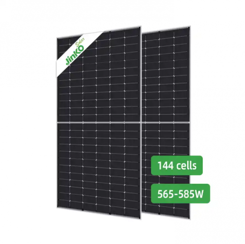
Evo 5 Series 144 Half Cells 555W 560W 565W 570 Wp 575 Watt Solar PV Panels N-type TOPCon Monocrystalline MBB Bifacial Double Side Glass Photovoltaic Solar Panel Module Based on 182mm Solar Cell
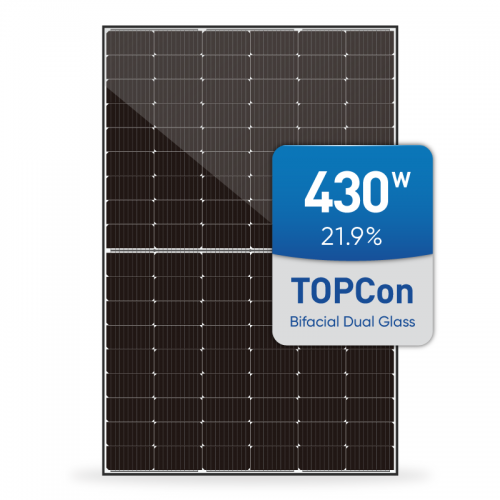
Evo 5 Pro Series 108 Half Cells 430W 425W 420W 415W 410 Watt Solar PV Panels N-type TOPCon Monocrystalline MBB Bifacial Double Side Glass Photovoltaic Solar Panel Module Based on 182mm Solar Cell
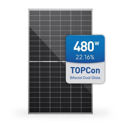
EVO 5N Series Bifacial modules combine leading N-type TOPCon technology, adapt 182mm silicon wafer and 16BB half-cell, 120 cells. The power output range is 460W 465W 470W 475W 480W.
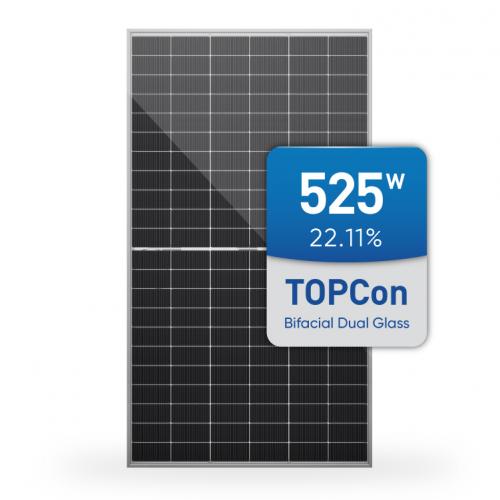
EVO 5N Series Bifacial modules combine leading N-type TOPCon technology, 182mm silicon wafer, and 16BB half-cell. The SunEvo N-type Bifacial Half-cell Module can reach a power output of range between 505W to 525W.
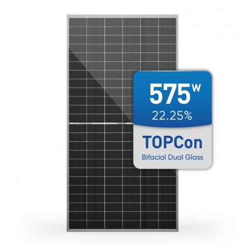
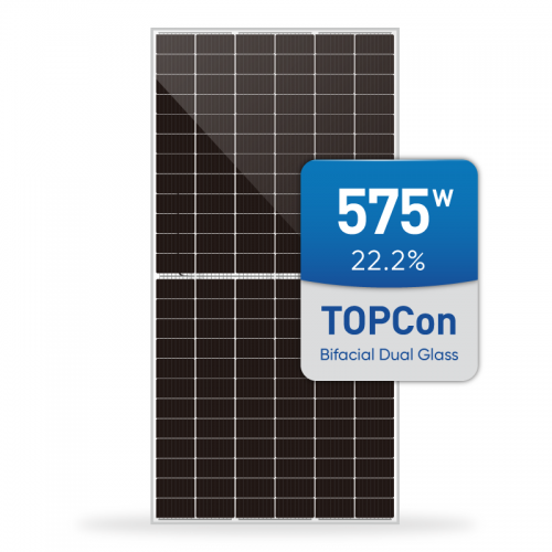
EVO 5N Series Bifacial modules combine leading N-type TOPCon technology, 182mm silicon wafer, and 16BB half-cell. Higher power generation under working conditions, thanks to passivating contact cell technology. The SunEvo N-type Bifacial Half-cell Module can reach a power output range between 555W to 575W.
The Tiger Neo N-type 72HL4-(V) model from JinkoSolar incorporates Hot 2.0 technology for enhanced light trapping, current collection, and overall module power output, ensuring superior reliability with lower LID/LETID. Its optimized mass-production process and materials control guarantee excellent Anti-PID performance, while also demonstrating high resistance to salt mist and ammonia exposure.
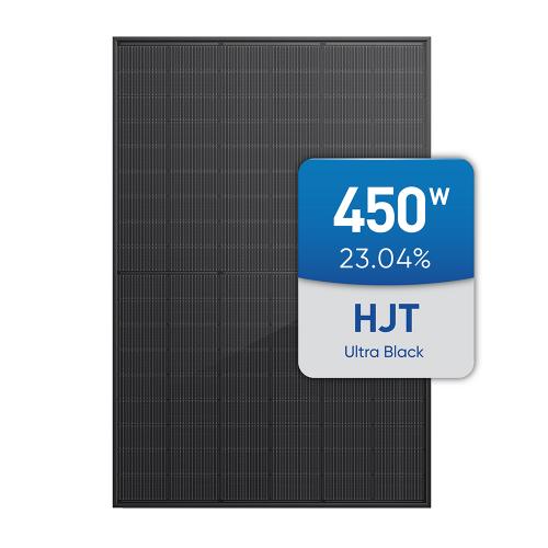
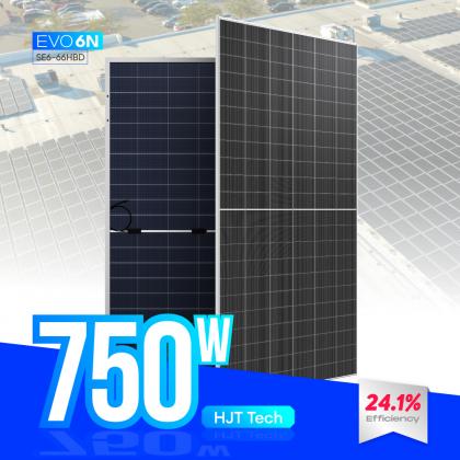
EVO 5N Series HJT (Heterojunction with Intrinsic Thin-layer) technology combines the advantages of crystalline silicon and thin-film solar cells, resulting in a remarkably high energy conversion efficiency. HJT All-Black panels can harness more sunlight and generate more electricity per square meter.
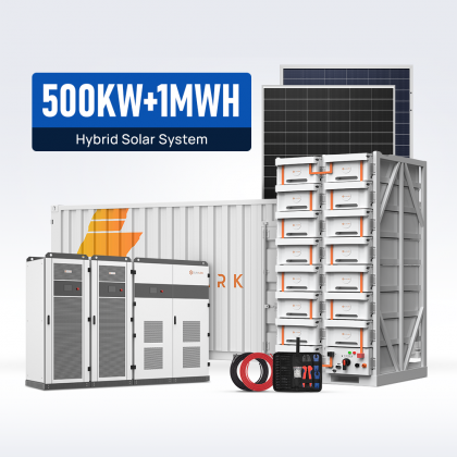
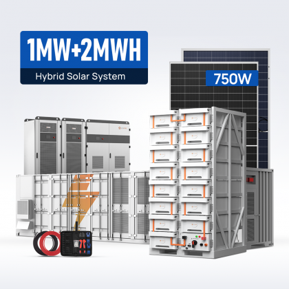
The solar energy storage system improves the user's self-use rate and brings greater benefits; currently the self-use part of the user's photovoltaic system is relatively low, perhaps less than 30%, and the combination of photovoltaic + energy storage will greatly provide spontaneous self-use ratio, thereby increasing user income.


 IPv6 network supported

 français
 Deutsch
 italiano
 español
 português
 العربية
 日本語
日本語 Polski
 ไทย
ไทย